2014/2015 represents the tenth anniversary of modern graphene research. Over this decade, graphene has proven to be attractive for thin-film transistors owing to its remarkable electronic, optical, mechanical and thermal properties. Even its major drawback—zero bandgap—has resulted in something positive: a resurgence of interest in two-dimensional semiconductors, such as dichalcogenides and buckled nanomaterials with sizeable bandgaps. With the discovery of hexagonal boron nitride as an ideal dielectric, the materials are now in place to advance integrated flexible nanoelectronics, which uniquely take advantage of the unmatched portfolio of properties of two-dimensional crystals, beyond the capability of conventional thin films for ubiquitous flexible systems.

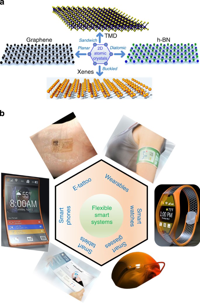
Two-dimensional (2D) atomic sheets are atomically thin, layered crystalline solids with the defining characteristics of intralayer covalent bonding and interlayer van der Waals bonding 1,2,3 . The expanding portfolio of atomic sheets illustrated in Fig. 1a currently include the archetypical 2D crystal graphene 3,4,5,6,7,8,9,10,11,12,13,14 , transition metal dichalcogenides (TMDs) 1,2,15,16,17,18,19,20,21 , diatomic hexagonal boron nitride (h-BN) 3,22,23,24,25 , and emerging monoatomic buckled crystals collectively termed Xenes, which include silicene 2,26,27 , germanene 2 and phosphorene 28,29,30,31 . These materials are considered 2D because they represent the thinnest unsupported crystalline solids that can be realized, possess no dangling surface bonds and show superior intralayer (versus interlayer) transport of fundamental excitations (charge, heat, spin and light). The portfolio is expected to grow as more elemental and compound sheets are uncovered.
The outstanding properties of 2D crystals have generated immense interest for both conventional semiconductor technology and the nascent flexible nanotechnology because, amongst other considerations, these atomic sheets afford the ultimate thickness scalability desired in a variety of essential material categories, including semiconductors, insulators, transparent conductors and transducers 3,16,18 . In particular, flexible nanoelectronics stand to greatly benefit from the development of 2D crystals because their unmatched combination of device physics and device mechanics is accessible on soft polymeric or plastic substrates 17,18,32,33 , which can enable the long sought after large-area high-performance flexible devices that can be manufactured at economically viable scales. As a result, existing flexible technology is expected to be transformed from low-cost commodity applications, such as radio-frequency identification tags and sensors, to integrated nanosystems with electronic performance comparable to silicon devices, in addition to affording mechanical flexibility and manufacturing form-factor beyond the capability of conventional semiconductor technology 34 . Hence, a new era in integrated flexible technology founded on 2D crystals is emerging.
This article serves as a general, albeit focused, review of flexible 2D nanoelectronics covering their progress, prospects and contemporary challenges. Remarkably, in the 10 years since basic academic studies of small graphene flakes was pioneered, commercial products are now available including smart phones with graphene touch panels. In general, 2D atomic sheets are under rapid development leveraging the understanding gained from graphene.
One might wonder: why flexible nanoelectronics? Can ubiquitous silicon electronics not fulfil the evolving technology aspirations of modern society? For some new technologies at the forefront of the innovation horizon, 2D atomic sheets offer a unique and compelling capability. A case in point is wearable electronics such as smart glasses, smart watches, smart fabrics and electronic tattoos 35 , which ideally require large-area nanomanufacturing of devices based on ultra-thin functional materials that are transparent and energy efficient, and can afford radio-frequency (RF) wireless connectivity on a flexible substrate. Another new example is an integrated communication and computation system, such as a universal ultra-portable gadget that can transform into several user-reconfigurable form factors including a smart phone, smart tablet and computer with the desirable benefits of low-cost manufacturing on soft substrates that are foldable, rollable, environmentally benign and recyclable. This sort of universal gadget has attracted the imagination of technology companies, embodied by Nokia’s ‘Morph’ concept 34 . In addition, the applications of 2D atomic sheets towards other emerging concepts, such as origami inspired foldable systems, flexible bioelectronics and wireless structural health monitors, could also substantially benefit from the atomic profile and high-performance transport properties. For clarity, we note that a ‘smart system’ can be understood simply as any gadget with embedded wireless connectivity that at a minimum can interact with the user or environment. Examples of some highly anticipated flexible smart systems are shown in Fig. 1b.
Historically, organic, amorphous and metal oxide thin-film transistors (TFTs) have been explored for flexible electronics; however, their low charge mobility (μ) has limited their prospects to specific low-frequency applications such as tags and control electronics for displays 34 . Figure 2 compares the charge mobility of several candidate semiconducting materials, clearly demonstrating that large-bandgap TMDs (for example, MoS2 and WSe2) offer experimental mobilities approaching single-crystal silicon TFTs, with two orders of magnitude thinner profile and higher strain limits. Encouragingly, recent reports have shown that another 2D semiconductor, phosphorene, can afford even higher transistor mobilities around 1,000 cm 2 V −1 s −1 at room temperature 28 , a significant advancement for TFTs. The mobility of TFT materials is of great interest because it influences several performance metrics, such as current density, energy efficiency, switching delay and cutoff or transit frequency (fT), a critical parameter for realizing GHz wireless connectivity. At low electric fields, the intrinsic fT=μEDS/(2πL), where L is the transistor channel length and EDS is the drain-source lateral electric field described by EDS=VDS/L within the gradual channel approximation 36 . VDS is the drain-source voltage. It follows that the charge mobility directly determines the low-power frequency capability and the likely applications comprising connectivity, communication and computation that can be realized in practice.
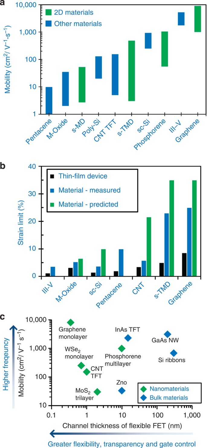
Achieving high mobilities in films that are atomically thin (Fig. 2c) is also noteworthy because the 2D thickness limit represents the ideal conditions for realizing maximum electrostatic control 16 , maximum optical transparency 6,18,37 , maximum chemical sensor sensitivity 1 and maximum mechanical flexibility 7,20,32 .
In Fig. 2, it can be seen that graphene affords the highest field-effect transistor (FET) mobilities, owing to its small effective mass (m*). However, the lack of a bandgap and the associated inability to electrically switch off precludes its use for digital transistors 4 . Nevertheless, its high charge mobility and saturation velocity (>10 7 cm s −1 ) coupled with its intrinsic ambipolar character make it an attractive material for flexible RF analogue TFTs 32,38 , which have already been employed to demonstrate several RF circuit blocks such as frequency multipliers 39 , and multi-modulation wireless circuits 37 . In addition, non-transistor applications including transparent conductive films, heat spreaders, acoustic speakers and mechanical actuators can all be enabled by flexible graphene, where the lack of a bandgap is not a limitation.
Table 1 summarizes the basic optical, electrical, mechanical and thermal properties of several 2D atomic sheets that span the range from semimetals to insulators. This table is a useful reference for guiding the selection of material(s) and device design for flexible nanoelectronics. As a general material, graphene offers the fastest charge transport, stiffness and thermal conductivity. Phosphorene and semiconducting TMDs are well suited to serve as the semiconducting channel for digital electronics. In addition, direct bandgap monolayer TMDs can be used for optoelectronics. For atomically thin insulating sheets, multilayer h-BN has been proven to be the ideal dielectric for enhanced charge transport for 2D TFTs, owing to its atomically smooth surface, large phonon energies, high dielectric breakdown field and high in-plane thermal conductivity compared with conventional dielectrics 3,18,39 .
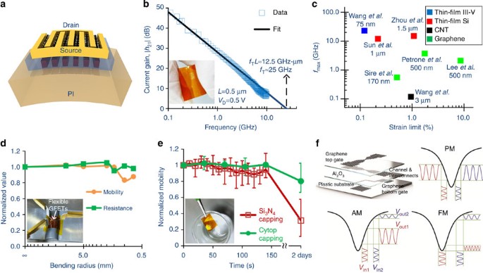
Graphene TFTs employing the embedded-gate structure with a 500-nm channel length have achieved intrinsic fT ∼ 25 GHz at a modest lateral field of 1 V μm −1 on plastics (Fig. 3b) 32 , corresponding to fT L ∼ 12.5 GHz-μm, the current state-of-the-art for flexible graphene. This result compares favourably with fT ∼ 53 GHz at a similar channel length on crystalline SiC substrate 57 at a much higher field of ∼ 4.5 V μm −1 . Increased lateral fields on flexible substrates should in principle afford commensurate increases in fT. However, the associated Joule heating can lead to channel peak temperatures that exceed the glass transition temperature (Tg) of soft substrates (Tg ∼ 350–400 °C for polyimide (PI), lower temperatures for other plastic substrates), resulting in local deformation of the plastic and ensuing device damage. This irreversible damage limits investigation of the ultimate high-field performance of high-mobility TFTs on plastic substrates, an issue that has only recently been brought to light 58 . We shall discuss the thermal management challenge in a later section.
An equally important frequency metric is the so-called maximum frequency of oscillation, fmax. While fT can be viewed as the upper frequency limit on the amplification of elementary electronic signals (for example, current), fmax can be interpreted as the upper frequency limit for achieving power gain. An eloquent discussion of these two frequency metrics can be found in the review article by Schwierz 4 . In general, simultaneously achieving both high fT and fmax is essential for analogue and RF electronics. In addition, fT and fmax should be (approximately) greater than 3–5 × the desired operating circuit frequency. Figure 3c shows a graphene TFT with extrinsic fmax ∼ 3.7 GHz (ref. 38). The true intrinsic fmax, commonly obtained by de-embedding the measurement probe pad parasitics, is likely higher. Promisingly, the high experimental fT and ongoing efforts to improve fmax into the microwave regime by contact and gate resistance reduction paints a positive prospect for graphene TFTs to enable future smart flexible systems with wireless connectivity. Experimental results on rigid (diamond-like carbon) substrates supports this optimism, with reported fT and fmax of about 120 and 45 GHz, respectively, an fT/fmax ratio ∼ 2.7 at a modest channel length of ∼ 150 nm (ref. 14). Further improvements of the frequency response have been achieved at sub-100-nm channel lengths by using physically transferred gate stacks 56 .
Regarding mechanical flexibility, tensile strains of up to 8% have been applied to high-frequency graphene TFTs 32,59 , which is substantially larger than what has been achieved with thin-film Si and III–V flexible transistors (Fig. 3c). Figure 3d details the electromechanical robustness of the mobility and contact resistance of a graphene TFT down to a bending radius of 0.7 mm. Even higher strains are expected to be possible since the intrinsic breaking strain of graphene is >20% (see Table 1).
Furthermore, several encapsulation coatings have been explored to improve the robustness of embedded-gate flexible graphene TFTs immersed in water or subjected to harsh conditions. The motivation for this type of investigation is that future smart systems have to be designed from the bottom-up to withstand common harsh conditions such as liquid spills and drops. Lee et al. 32 determined that a top-side bilayer coating of a hydrophobic fluoropolymer and a chemically inert silicon nitride diffusion barrier coupled with the low moisture absorption of PI substrate can provide effective protection against continuous immersion in water for up to 2 days (Fig. 3e).
By taking advantage of the unique ambipolar properties of graphene, several workers have demonstrated reconfigurable modulation circuits useful for wireless communication systems 37,39 . One particular example by Zhong and coworkers 37 is shown in Fig. 3f, in which a flexible all-graphene circuit on a transparent plastic sheet was employed to achieve three information modulation schemes: amplitude, phase and frequency modulation that would otherwise take a more complex circuit based on conventional semiconductors to realize.
A primary limitation of graphene is the strength of semiconducting TMDs; the sizeable bandgap exhibited by TMDs affords near ideal electronic switches with on/off current ratios typically exceeding seven orders of magnitude. Combined with thickness scalability down to a monolayer that allows ideal electrostatic switches, TMDs are highly attractive for flexible digital electronics 1,2,16 . Early work on monolayer and multilayer flexible TMD transistors, mostly exploring MoS2 TFTs, has been encouraging 17,18,60 . Figure 4a shows the electronic performance of a bendable n-type MoS2 TFT on PI with integrated high-k dielectric in a back-gated device structure featuring on/off ratio >10 7 and near ideal sub-threshold slope. The device low-field carrier mobility and contact resistance are ∼ 30 cm 2 V −1 s −1 and 2 TFTs are still several times lower than that of comparable state-of-the-art devices on hard Si substrates 15 . This might be related to several factors, including the optimum film thickness and dielectric environment, in addition to differences in material quality and residual stresses.
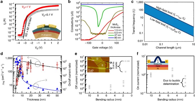
For optoelectronic devices, monolayer thick ( ∼ 0.7 nm) semiconducting TMDs are preferred, owing to their direct bandgap character 1 . However, for transistor electronics, the optimum number of layers for the usual device parameters of interest, such as carrier mobility, current drive, contact resistance and electrostatic control, remains unclear. In this context, Appenzeller and coworkers 15 investigated unpassivated MoS2 back-gated devices on SiO2/Si and concluded that films around 10 nm thickness offered the highest mobility ( ∼ 184 cm 2 V −1 s −1 ), owing to competing effects of interface screening and interlayer resistance. In contrast, Fuhrer and coworkers 62 evaluated multilayer MoS2 TFTs with a polymer back-gate dielectric surrounding and found that ∼ 47 nm thick film yielded the highest mobility ( ∼ 480 cm 2 V −1 s −1 ) in their experimental study. Separate work by Javey and coworkers 16 demonstrated that a single layer of WSe2 in a top-gated device structure can yield higher mobility ( ∼ 250 cm 2 V −1 s −1 ) than reported for few-layer MoS2.
Though differences in effective mass is a factor in carrier transport (W-TMDs have a lower effective mass than Mo-TMDs), theoretical studies by Ma and Jena 63 indicate that charged impurities and the effect of the top and bottom dielectric environment are prominent factors in contemporary experimental devices. Indeed, comparing the results of Appenzeller and Fuhrer suggests that is the case with TMD thickness and dielectric environment significantly influencing mobility and charge transport in fabricated TFTs. Intriguingly, the polymer environment on the thick MoS2 device also afforded almost symmetric ambipolar electron and hole transport (Fig. 4b), a fairly rare occurrence for MoS2 transistors. The inconclusive nature of experimental findings to date calls for continued investigation of TMD TFTs to further elucidate on the device physics and structures for accessing their maximum electronic performance.
A topic related to 2D materials that has yet to be thoroughly considered for the case of TMDs is the likely tradeoff between carrier mobility and the minimum contact resistance due to their opposite dependence on effective mass. On one hand, low effective mass is desirable for fast transport (μ ∝ 1/m ) . However, low effective mass also translates to low density of states, hence increasing the minimum contact resistance () 64 due to the reduced availability of states for charge injection. To the extent that this tradeoff holds true in scaled experimental devices (that is, extrinsic factors do not dominate the transport or contacts), then it might not be straightforward to directly determine the most suitable semiconducting TMD simply based on mobility alone. Additional studies are needed to shed light on the conditions for optimizing charge injection and transport.
High-frequency transport in 2D semiconducting crystals is an important performance metric for high-speed digital and RF electronics. Theoretical estimates for the intrinsic fT can be derived from classical semiconductor physics based on the velocity (v) model, , (refs 27, 36).
where the former term within the bracket defines the low-field limit and the latter term sets the high-field limit, governed by velocity saturation (vsat). For low-power nanoelectronics, constant-field (EDS) channel length scaling leads to a fT ∝ 1/L dependence in both the low- and high-field limits. It is worthwhile to note that equation (1) depends on two material properties, low-field μ and vsat, and can be universally applied to the portfolio of semiconducting 2D crystals. To gauge the range of intrinsic fT that can be expected from TMD TFTs, we examine the case of a modest mobility (μ ∼ 30 cm 2 V −1 s −1 ) for the low-end low-field limit, and a theoretically estimated vsat ∼ 4 × 10 6 cm s −1 (ref. 27) for the high-end high-field limit. Under this treatment, the expected fT performance range is shown in Fig. 4c, essentially reflecting all mobility values above the low-end value and all velocities below the high-end value. It follows that the two limiting cases translate to two important performance values, fTL ∼ 0.4 GHz-μm and fTL ∼ 6 GHz-μm, for the low-end and high-end frequency performances, respectively. For channel lengths in the 100–250 nm range, the high-field fT is in the microwave band, which is sufficient to realize high-speed digital and GHz circuits. Phosphorene offers mobilities as high as 1,000 cm 2 V −1 s −1 (Fig. 4d) 28 which will lead to higher intrinsic frequency performance compared to semiconducting TMDs. Indeed, phosphorene might very well be the most promising of the current portfolio of 2D semiconductors owing to its higher mobility while affording a suitable band gap 28,31 .
However, to access the full high-frequency capability of 2D semiconductors, the effects of contact resistance, charge impurities and remote phonon scattering are detrimental device parameters that need to be minimized.
Regarding mechanical flexibility, the limited studies on device mechanics have introduced an additional constraint relating to the question on the optimum thickness for flexible nanoelectronics. Chang et al. 17 evaluated the bendability of back-gated MoS2 TFTs and found that the TFTs were robust down to a few mm bending radius followed by device failure initiated by two distinct thin-film mechanics 58 , namely: (i) cracks in the dielectrics were responsible for off current degradation (Fig. 4e) and (ii) buckle delamination resulted in on current degradation as shown in Fig. 4f. The former can be mitigated by patterning the dielectric into islands, as has been demonstrated for graphene TFTs 59 or using ion-gel gate dielectrics 60 .
Buckle delamination of MoS2 shows a quasi-linear dependence of the buckling height on the film thickness 58 , which can be attributed to the thickness dependence of the buckling driving force. It follows that a monolayer TFT is preferred from a device mechanics point of view, in contrast to the conclusion from mobility considerations that indicate a few layers are optimum 15 , thereby suggesting a tradeoff in the number of layers that afford optimum device physics and device mechanics. This tradeoff might be mitigated by using high-quality h-BN gate dielectric where its atomic smoothness and high phonon energy are expected to enhance monolayer TMD mobilities as is the case for graphene 3,9 . Beyond bending studies, hydrostatic compressive strain of MoS2 of about 15% has been recently reported to produce a semiconducting to metallic transition, which can enable new flexible or straintronic device or switch concepts 65 .
Heterostructures composed of different atomic layers have been recently recognized as a new playground for material designers where the desired composite properties can be tailored and the whole can potentially be greater than the sum of its parts 1,2,9,66 . Synthesizing or preparing 2D heterostructures is currently a major research activity with increasing worldwide interest because of the seemingly unlimited range of application prospects. 2D heterostructures can enable flexible and transparent electronic, memory, optical, sensor and energy conversion devices. Recent work on soft substrates has focused on graphene-, h-BN- and TMD-layered heterostructures for flexible device applications 18,39,66 . The simplest and perhaps the most obvious heterostructure is a bilayer consisting of a stacked channel and dielectric such as graphene and its ideal dielectric, h-BN. The high phonon energies and thermal conductivity of h-BN can result in mobility enhancement and improved electronic performance 3,9,13 . For this reason, Lee et al. 39 realized a flexible device based on a monolayer graphene—multilayer h-BN heterostructure, which resulted in record 2D TFT current densities on plastics (Fig. 5a).
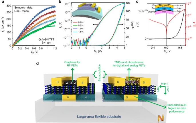
The next evolutionary development is a trilayer heterostructure that can draw from the individual properties of three different atomic nanomaterials, such as TMD semiconductors, h-BN dielectrics and graphene electrodes. This offers the advantage of an intrinsically transparent transistor that benefits from the low absorption of the individual layers as demonstrated recently on polyethylene naphthalate (PEN) substrates 18 (Fig. 5b). Moreover, the source and drain electrodes that are typically metals can be replaced with single or few-layer graphene as contacts, which not only enables a fully transparent TFT but also improves the overall device flexibility and provides contact tunability of the graphene-channel Schottky barrier resulting in reconfigurable n- or p-type TFTs 33 .
For field-effect tunnelling transistors, more complex 2D heterostructures are needed if one aims to realize the entire stack with layered materials. Mishchenko and co-workers 66 achieved this feat by sequential exfoliation and transfer of five different layers with graphite serving as the gate, h-BN as the dielectric, few-layer WS2 electron tunnel barrier and monolayer graphene contacts, as illustrated in Fig. 5c. As materials growth advances, integration of layered sheets for heterostructure realization will become more manufacturable and enable comprehensive studies for flexible nanoelectronics.
In light of the outstanding potential for 2D atomic sheets for advanced flexible nanoelectronics, it is prudent to balance this perspective with a discussion of the pressing challenges that need to be addressed before Si-like large-scale integration and performance can be realized on soft substrates. Foremost amongst these challenges is the need for research and development of complementary n- and p-type 2D transistors. Complementary transistor technology has been the foundation of modern low-power integrated electronics for the past five decades. Any practical vision for integrated flexible smart systems will require complementary TFTs for essential circuits, including bias circuitry, data converters, signal processing blocks and microprocessors.
Much of the progress on semiconducting atomic sheets have so far found that intrinsic 2D semiconductors typically exhibit either n- or p-type device transport 1,2,15,16,67 , instead of ambipolar behaviour expected in the absence of intentional doping 68 . A case in point is MoS2 and MoSe2, which typically afford n-type FETs, even when high work function contacts that should theoretically favour hole transport are used 1,12,67 . Likewise, WSe2 and phosphorene typically afford p-type FETs 16,28,31 . For TMDs, this observation has been attributed to a variety of factors including Fermi level pinning at the contacts 15 and material defects such as vacancies or interstitials that can result in n- or p-type defect levels 69 . Also, one can expect contaminants and adsorbates from the ambient and lithography process to influence the device polarity, in addition to the observed effects of certain dielectric interfaces (for example, polymeric or ion-gel dielectrics), which are not yet well understood 60,62 . Clearly, sustained research is warranted in terms of synthesizing high-purity materials with negligible defects and continued studies in understanding the contact—2D and dielectric—2D interfaces to achieve the desired carrier transport.
It should be noted that conventional substitutional doping of the 2D semiconductor channel is generally not envisioned as a viable technique for controlling carrier type, owing to the high likelihood of crystal damage and mobility reduction. Similar to the case of semiconducting carbon nanotubes, contact engineering is regarded as a suitable method based on low or high work function electrode interfaces to obtain n- and p-type FETs, respectively 12 . Moreover, the gate electrode can be selected to tune the threshold voltage. Alternatively, self-assembled monolayers can be applied to polymer substrates to effectively dope overlaying graphene layers 70 . Such doping can be spatially controlled by patterning of the self-assembled monolayers.
Soft substrates cannot tolerate heat compared with bulk semiconductors or ceramics that typically have melting temperatures much higher than practical device operating temperatures. For this reason, thermal management is a more pronounced challenge for flexible electronics, particularly for 2D channel materials in which high current densities needed for the maximum speeds can lead to peak temperatures that are comparable to or can exceed the glass transition temperature of plastic substrates. In the case of graphene, channel hotspots from Joule heating can exceed 300 °C (ref. 71), which results in plastic substrate deformation and irreversible device damage 58 (Fig. 6a). Typical power density limits for bottom-gated GFETs are ∼ 20 kW cm −2 (0.2 mW μm −2 ) and ∼ 45 kW cm −2 on PEN and PI substrates, respectively. Overcoming the heat barrier requires use of thermal management materials to prevent the substrate from experiencing temperatures beyond its reliable limit. It is significant to note that the overall RF performance (for example, gain and cutoff frequencies) of flexible graphene TFTs is ultimately limited by thermal constraints of the substrate rather than by electronic characteristics of the device.

Unlike conventional electronics where the substrate is thermally conductive and metallic heat sinks can be used, most flexible substrates are poor thermal conductors, and there is very limited research on strategies for thermal management. Lee et al. 58 proposed employing h-BN for thermal management, because its anisotropic thermal properties (Table 1) appear to be ideal for in-plane heat spreading to metal contacts and out-of-plane heat isolation as depicted in Fig. 5d. The main question regards the minimum h-BN thickness required to ensure that the substrate stays within its reliable temperature range during high-field TFT operation. In general, the minimum h-BN thickness will depend on the maximum channel temperature, channel thermal conductivity, channel—h-BN thermal interface resistance, substrate Tg, radiation efficiency to the ambient and channel length, with shorter channels providing increased assistance in heat spreading to the contacts. An alternative material stack that achieves a similar goal of anisotropic thermal management can be constructed from a bilayer film with thermally conductive (for example, BeO) and insulating thin layers facing the hot channel and soft substrate, respectively. Ongoing research on thermal management for flexible nanoelectronics is expected to provide guidance for reliable device design and optimum operation.
Large-scale nanomanufacturing of 2D thin films and devices on soft substrates is an essential prerequisite for practical flexible nanoelectronics. In this regard, much of the public and technical imagination has focused on nanomanufacturing based on sheet or roll-to-roll (R2R) processing 72,73 for large-area or high-volume nanotechnology that can be as ubiquitous as modern Si very large-scale integration. Either nanomanufacturing method will be rather complex, involving material growth, transfer and lithography in a benign manner to minimize contamination and defects (Fig. 6b). Defects present in 2D semiconductors and dielectrics grown by chemical vapour deposition and subsequently transferred onto process substrates encompass: (i) growth-related crystal imperfections such as vacancies, interstitials, grain boundaries and slip planes in multilayer films and (ii) process related defects such as wrinkles, bubbles, tears and chemical contamination.
For the manufacturing of graphene, large-area growth and R2R processing has experienced substantial progress in the last few years 55,56 , as depicted in Fig. 7a,b showing the state-of-the-art in graphene R2R that has enabled 100 m long transparent conductive rolls 73 . Indeed, graphene has recently penetrated the consumer market replacing indium tin oxide as the touch screen panel in some smart phone products in China (Fig. 7c). The current flexible technology maturity of 2D sheets is summarized in Fig. 7e revealing several demonstrated advances of large-area graphene in contrast to the emerging 2D nanomaterials which are still at a nascent stage. We expect that much of the progress in graphene R2R development will benefit the nanomanufacturing of other 2D atomic sheets with substantial advancement needed in terms of: (i) understanding and minimizing crystal grain boundaries, defects and doping 1,2,69 and (ii) development of large-area growth techniques and benign transfer integration onto soft substrates 2 . It is worth noting that current graphene R2R transfer is based on the complete etching of copper foils, a scheme that may be unsustainable for cost, scale, or waste processing reasons. Alternative transfer methods that show strong promise include electrochemical and dry delamination, both of which preserve the foil for reuse 74,75 . Figure 7d demonstrates recent electrochemical delamination of graphene directly onto PI.
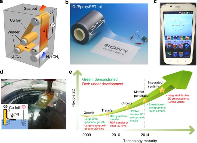
Direct growth or integration of assorted layers of 2D semiconductors, dielectrics and conductors is of course the ideal method for realizing high-performance integrated flexible smart systems, which is a grand technology vision for 2D materials as stated in Fig. 7e. We anticipate that flexible smart systems will likely be commercial products over the next 10 years based on the rapid progress so far, which is generally in-line with the time frame of the 10-year EU Graphene-Flagship project ( http://graphene-flagship.eu/).
We note that carbon nanotube is another candidate nanomaterial that is under development for flexible nanotechnology. Nanotube smart phone touch panels (produced by Tianjin’s CNTouch (http://www.cntouch.com/) in China) have also recently penetrated the consumer market in 2014 and directly competes with graphene as an indium tin oxide replacement. Moreover, flexible integrated systems based on nanotubes have been demonstrated 12,76,77 ; however, it is too early to determine how nanotubes will fare with 2D films for commercial flexible systems. At present, graphene has experienced a more rapid large-scale development in transitioning into the touch panel market given that nanotubes have been researched for longer. The challenge facing nanotubes produced by large-scale manufacturing is the need for both high tube density and carrier mobilities while affording sufficiently large on/off ratios for high-performance transistors 12 , a long-standing research topic.
We conclude by noting that research on flexible 2D atomic sheets began only a few years ago, with the first papers on flexible graphene, flexible TMD and phosphorene transistors in 2007, 2012 and 2014, respectively. In this time frame, the achieved electronic performance has already substantially exceeded those of organic, amorphous and metal oxide thin-film transistors that have enjoyed decades of research activity. The remarkable high mobility of few-layer phosphorene, which is superior to that of TMDs and silicon TFTs could have a transformational impact in enabling flexible high-performance electronics. The recent graphene penetration of the consumer smart phone market is a major milestone and could be a launch pad for the development of large-scale active electronics. The path to further commercialization is, of course, not exactly predictable. However, sustained research effort that address the major challenges will be indispensable in translating the potential of 2D nanomaterials into a practical high-performance flexible ubiquitous nanotechnology.
How to cite this article: Akinwande, D. et al. Two-dimensional flexible nanoelectronics. Nat. Commun. 5:5678 doi: 10.1038/ncomms6678 (2014).
This work is supported in part by the Office of Naval Research (ONR) under contract N00014-1110190, the Defense Advanced Research Projects Agency (DARPA) under ONR contract N00014-1210814 and the National Science Foundation (NSF) NASCENT Nanosystems Engineering Research Center under Cooperative Agreement No. EEC-1160494. We acknowledge helpful discussions with our current and former researchers, including Dr Li Tao, Dr Jongho Lee, Hsiao-Yu (Sherry) Chang and Weinan Zhu.